Advanced Functions for Semiconductor Metrology

The AM (Automated Measurement) module adds advanced semiconductor metrology functions to the Quartz PCI software that automate feature measurements in electron microscope images.
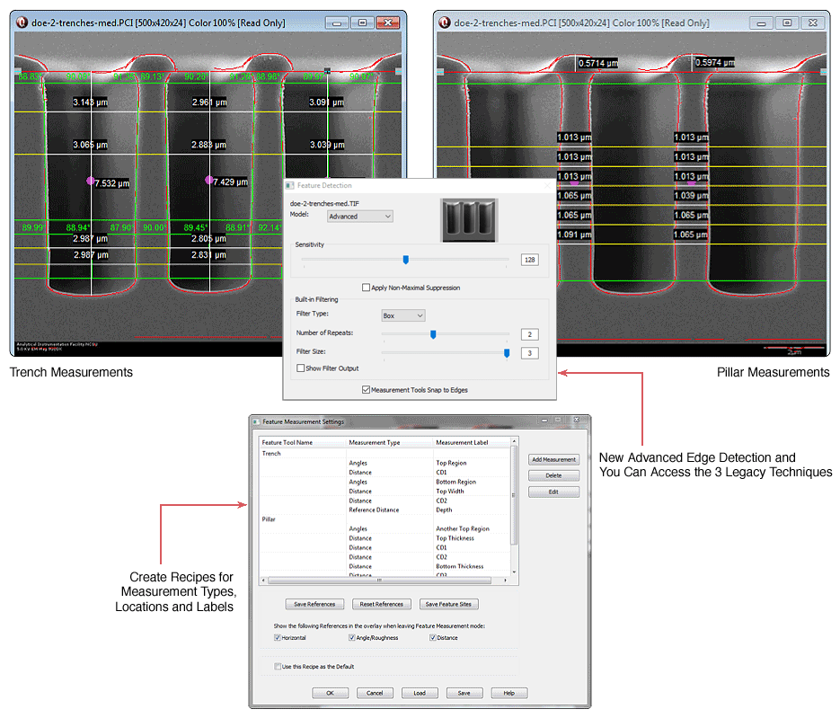
Unlike tools designed for in-line metrology using top view images such as CD-SEMs, PCI-AM is particularly well suited for measuring semiconductor features in cross-section and top view images from SEMs (X-SEM) and TEMs in laboratory, process development and engineering environments. Multiple edge detection techniques are employed depending on the nature and source of the image.
Very little set-up is required before you can be making fast, efficient automatic image measurements.
What's NEW in QUARTZ PCI-AM 8
- Improved Edge Detection – better edge detection, particularly for TEM images
- Image Auto Rotation – automatically orient features horizontally and vertically for ease of measurement
- Measurement Tolerances – measurements can be checked against user-specified tolerances
- Auto Layer Detection and Measurement – if needed these lines can be moved
- Add Additional Reference Lines – assist in making desired measurements
Semiconductor Features
Tools are provided for automatically measuring layers, trenches, pillars, lines, spaces, complex features and 2D shapes, such as contact holes and vias. Within these features, you can measure widths and heights (critical dimensions), sidewall and center angles (in multiple regions), edge roughnesses, line width roughnesses, and other geometric properties.
Edge Detection
Three different edge detection techniques are available allowing analysis of both SEM and TEM images. Noise reduction filtering is also available to improve results with noisy images. A setting is also available that causes the standard Quartz PCI Image Measurement tools to snap to the detected edges.
Three Levels of Automation
The system offers three levels of automation. In the first instance, engineers simply click inside a device feature and the feature is automatically measured in accordance with a "recipe" that has been set up. In the second instance, once multiple features in an initial image have been measured, the same features can be measured in subsequent images with a single click. The system automatically adjusts for misalignment among the images. The third and newest level of automation allows engineers to automatically characterize an entire folder of images.
Benefits of Automatic Semiconductor Metrology
Save Time and More
With PCI-AM, dozens of semiconductor feature measurements on an image can be reduced to a single mouse click, resulting in very significant time savings versus manual measurements. In addition, inaccuracies and inconsistencies among engineers can be reduced. PCI-AM also simplifies data collection and aggregation through its options to export metrology data to spreadsheet files.
Data Collection
The measurement results are displayed on the image and in a spreadsheet grid. The data in the grid can be easily exported into a CSV file suitable for importation into other software such as Microsoft Excel allowing for further statistical analysis. Data from multiple images can be aggregated into a single spreadsheet file. The images and data can also be easily included in standard Quartz PCI reports with just a few clicks.
Custom Development
Quartz Imaging has a long history of providing specialized metrology solutions to the semiconductor industry. If you have unique measurement requirements, we would be delighted to discuss development of a custom metrology solution with you.
Quartz PCI-AM Automated Semiconductor Metrology System: Key Benefits
- Saves time for Engineers
- Ensures more accurate and consistent measurements
- Data export is very easy
- Quick report generation
- We can custom develop for your specific requirements